

A normal diode blocks current in reverse — until it is pushed too far, and then it breaks down and is usually destroyed. A Zener diode is the exception: it is deliberately designed to break down at a precise, predictable voltage and survive it. Once that voltage is reached, the diode holds its terminals at almost exactly that value no matter how much current flows through it. That single property makes the Zener diode the simplest voltage regulator in electronics — a two-component circuit that can turn a wobbly 12 V supply into a rock-steady 5.1 V for a sensor, a reference, or a low-power load.
This guide explains what a Zener diode is, how it works, how to read its VI curve, and how to design a working Zener voltage regulator with real numbers. If you are new to diodes, our guide to what a diode is covers the basics first, and our semiconductor guide explains the doped silicon it is made from.
What Is a Zener Diode?
A Zener diode is a silicon semiconductor diode with a heavily doped p-n junction, designed to operate in reverse breakdown at a precise voltage called the Zener voltage (Vz). In forward bias it behaves like an ordinary diode, conducting after about 0.7 V. In reverse bias it blocks current like any diode — until the reverse voltage reaches Vz. Then it starts conducting heavily in reverse, but the voltage across it stays almost constant at Vz even as the current rises sharply. That flat, constant-voltage region is the whole point of the device.
The effect is named after physicist Clarence Melvin Zener, who described the quantum tunneling mechanism behind it in 1934. Zener diodes are manufactured with Vz values from about 2.4 V up to 200 V, in power ratings from 0.25 W to 50 W, and they are sold by their Vz — a 1N4733A is a 5.1 V, 1 W Zener, for example. The circuit symbol is a diode with bent “wings” on the cathode bar, which marks it out from an ordinary diode on a schematic.
How a Zener Diode Works: Zener vs Avalanche Breakdown
Heavy doping makes the Zener diode’s depletion region very thin. When reverse voltage is applied, the electric field across that thin region becomes extremely strong, and two different breakdown mechanisms can take over, depending on the voltage:
- Zener breakdown (below about 5.6 V): the electric field is so intense that it pulls electrons directly through the depletion region by quantum tunneling. This is the true Zener effect. It has a negative temperature coefficient — Vz falls slightly as temperature rises.
- Avalanche breakdown (above about 5.6 V): charge carriers gain enough energy to knock more carriers free on collision, and the process multiplies like an avalanche. This has a positive temperature coefficient — Vz rises slightly with temperature.
At around 5.6 V the two effects balance out, so 5.6 V Zener diodes have a near-zero temperature coefficient — one reason the 5.1 V and 5.6 V values are so popular as voltage references. In practice, “Zener breakdown” is used as the general name for both mechanisms, and the datasheet simply gives you Vz, measured at a specified test current (IzT).
The key point for circuit design is that breakdown is controlled and non-destructive — as long as the current is limited by a series resistor so the power rating is not exceeded. An ordinary diode breaks down the same way, but at an uncontrolled voltage and with no guarantee of surviving it.

The Zener Diode VI Curve Explained
The voltage-current (VI) characteristic curve of a Zener diode has three regions, and reading it is the fastest way to understand the device:
- Forward region (first quadrant): the diode behaves like a normal silicon diode. Current stays near zero until about 0.7 V, then rises steeply. Nothing special happens here.
- Reverse leakage region: with reverse voltage below Vz, only a tiny leakage current (microamps) flows. The diode is effectively off.
- Breakdown region: at Vz — the “knee” of the curve — the current shoots upward while the voltage stays almost flat at Vz. The curve is nearly vertical here, which is exactly what a voltage regulator needs: large current changes produce almost no voltage change. The slope of this region is the diode’s dynamic resistance (rz), typically a few ohms to a few tens of ohms; a smaller rz means tighter regulation.
Two current limits matter. The minimum Zener current (Iz(min)), often around 1–5 mA, is the smallest current that keeps the diode in the flat breakdown region; below it, the diode slips out of regulation and the output voltage falls. The maximum Zener current (Iz(max)) is set by the power rating: Iz(max) = Pz(max) / Vz. Exceed it and the diode overheats and fails. Good design keeps the operating current between these two limits under all conditions.
Key Zener Diode Parameters
| Parameter | Symbol | Meaning | Typical Value |
|---|---|---|---|
| Zener (breakdown) voltage | Vz | Reverse voltage at which breakdown occurs, measured at the test current | 2.4 V to 200 V |
| Test current | IzT | Current at which Vz is specified on the datasheet | 5–50 mA |
| Minimum Zener current | Iz(min) | Lowest current that keeps the diode in regulation | 1–5 mA |
| Maximum Zener current | Iz(max) | Set by the power rating: Pz(max) / Vz | Depends on power rating |
| Maximum power dissipation | Pz(max) | Maximum power the diode can dissipate without overheating | 0.25 W, 0.5 W, 1 W, 5 W |
| Dynamic resistance | rz | Slope of the VI curve in breakdown; lower means better regulation | 2–50 Ω |
| Temperature coefficient | — | How much Vz drifts with temperature; near zero at ~5.6 V | Negative below 5.6 V, positive above |
Zener Diode as a Voltage Regulator
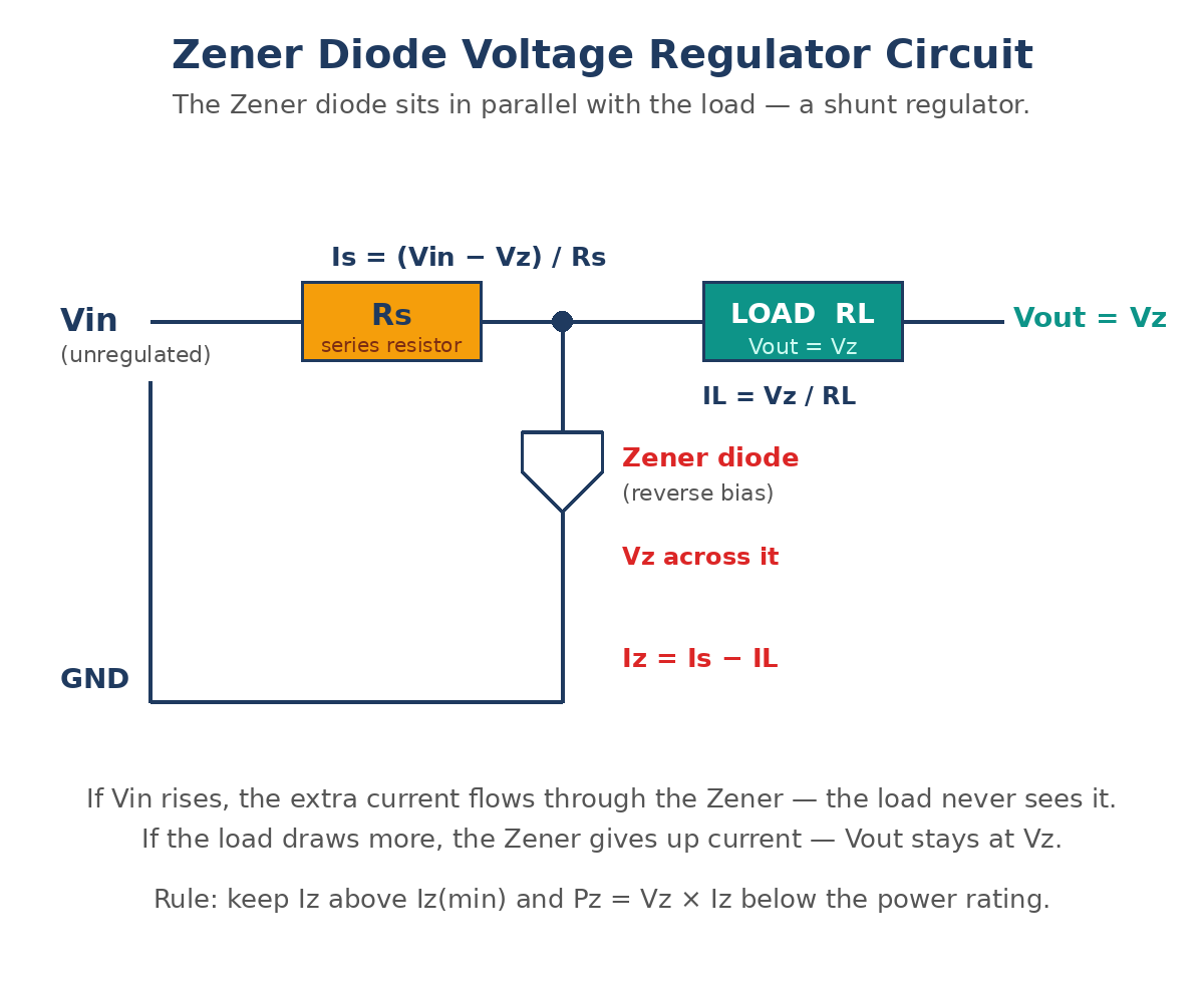
The classic Zener regulator is a shunt regulator: the Zener diode is connected in parallel (shunt) with the load, in reverse bias, with a series resistor (Rs) in front of it. The resistor drops the difference between the input and the Zener voltage, and the diode absorbs whatever current the load does not use. If the input voltage rises, the extra current flows through the Zener instead of the load, so the output stays at Vz. If the load draws more current, the Zener gives up some of its current, and again the output stays at Vz — as long as the Zener current never falls to zero.
The design rests on three formulas, all from Ohm’s law and Kirchhoff’s current law at the output node:
- Output voltage: Vout = Vz (while the diode is in breakdown)
- Series current: Is = (Vin − Vz) / Rs
- Zener current: Iz = Is − IL, where IL = Vz / RL is the load current
- Zener power: Pz = Vz × Iz — must stay below Pz(max)
Worked Example: Designing a 5.1 V Zener Regulator
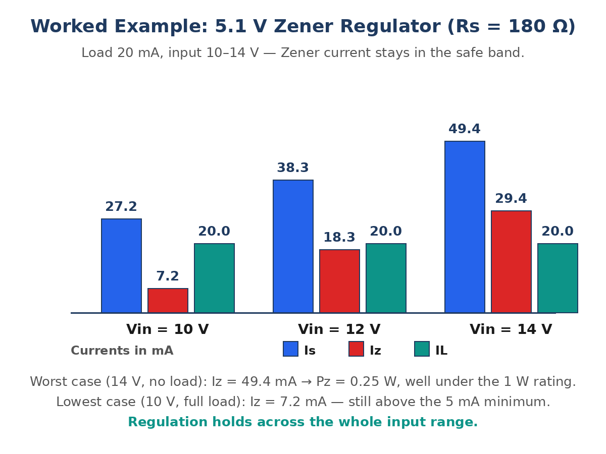
Let us design a regulator for a small sensor circuit. The requirements are: regulated output 5.1 V, load current up to 20 mA, input from an unregulated supply of 12 V nominal, ranging from 10 V to 14 V. We will use a 5.1 V Zener diode (such as the 1N4733A, rated 1 W) and assume a minimum Zener current of 5 mA to stay firmly in regulation.
Step 1 — choose the series resistor. Design for the worst case: the lowest input voltage (10 V) with the heaviest load (20 mA), because that is when the Zener current is smallest. The resistor must pass the load current plus the minimum Zener current:
- Rs = (Vin(min) − Vz) / (IL(max) + Iz(min)) = (10 − 5.1) / (0.020 + 0.005) = 4.9 / 0.025 = 196 Ω
Pick the nearest standard value below it, 180 Ω (a lower resistor gives slightly more Zener current, which is the safe direction). Check the resistor’s own power rating at the worst case — maximum input voltage with the load disconnected, when all the current flows through the resistor: Is = (14 − 5.1) / 180 = 49.4 mA, so PRs = (14 − 5.1) × 0.0494 = 0.44 W. Use a 1 W resistor for a comfortable margin.
Step 2 — verify regulation at the worst case. At minimum input (10 V) and maximum load (20 mA): Is = (10 − 5.1) / 180 = 27.2 mA, so Iz = 27.2 − 20 = 7.2 mA. That is above the 5 mA minimum, so the diode stays in breakdown and the output holds at 5.1 V. Regulation holds.
Step 3 — verify the diode survives the opposite extreme. At maximum input (14 V) with the load disconnected (IL = 0): Is = (14 − 5.1) / 180 = 49.4 mA, all of it through the Zener, so Pz = 5.1 × 0.0494 = 0.25 W. That is well under the 1 W rating of the 1N4733A. The design is safe.
Step 4 — check the nominal case. At 12 V input with the 20 mA load: Is = (12 − 5.1) / 180 = 38.3 mA, Iz = 38.3 − 20 = 18.3 mA, Pz = 5.1 × 0.0183 = 0.093 W. The diode runs cool and well inside its limits. The design works across the full input range and load range.
Where Zener Diodes Are Used
- Low-power voltage regulation: the classic use — a stable supply for sensors, reference circuits, and small loads where a few milliamps are enough. For higher currents, a Zener is usually paired with a transistor as a series regulator, or replaced by an IC regulator.
- Voltage references: a 5.6 V Zener (near-zero temperature drift) provides a stable reference for analog-to-digital converters, comparators, and test equipment.
- Overvoltage protection: a Zener across a sensitive input clamps any surge to Vz, protecting the circuit behind it — the same clamping idea used in surge protection, covered in our resistor guide‘s companion protection articles.
- Waveform clipping and shifting: back-to-back Zeners clip both halves of an AC waveform at a set level, and a single Zener shifts a signal’s DC level by Vz — useful in signal conditioning.
- Meter protection: Zeners across analog meter movements and measurement inputs clamp fault voltages before they can damage the instrument. The filtering capacitors around such circuits are covered in our capacitor guide.
Zener Diode vs Ordinary Diode
| Feature | Zener Diode | Ordinary (Rectifier) Diode |
|---|---|---|
| Designed operating region | Reverse breakdown | Forward conduction |
| Doping level | Heavily doped (thin depletion region) | Lightly doped |
| Breakdown voltage | Precise and specified (2.4–200 V) | High and unspecified (often 50–1,000 V) |
| Reverse breakdown | Controlled and non-destructive | Uncontrolled — usually destroys the diode |
| Main use | Voltage regulation and reference | Rectification (AC to DC) |
| VI curve | Sharp knee at Vz in reverse | Flat reverse region until failure |
Frequently Asked Questions
What is a Zener diode used for?
Mostly for voltage regulation and voltage reference. A Zener diode holds a constant voltage across its terminals in reverse breakdown, so it is used to stabilize low-power supplies, provide reference voltages, and protect circuits from overvoltage.
What is the difference between a Zener diode and a normal diode?
A normal diode is designed to conduct in forward bias and block in reverse; reverse breakdown destroys it. A Zener diode is heavily doped so it breaks down at a precise, specified voltage and survives it — that controlled breakdown is its whole purpose.
What is Zener voltage (Vz)?
The reverse voltage at which the Zener diode enters breakdown and starts conducting heavily while holding its voltage nearly constant. It is the diode’s defining specification, ranging from about 2.4 V to 200 V depending on the part.
How do I calculate the series resistor for a Zener regulator?
Use Rs = (Vin(min) − Vz) / (IL(max) + Iz(min)). Design for the lowest input voltage and the heaviest load, then check that the Zener power (Pz = Vz × Iz) stays below its rating at the highest input voltage with the load disconnected.
Can a Zener diode regulate high currents?
Not on its own — the diode would overheat, because all the unused current passes through it. For loads above a few tens of milliamps, use the Zener as a reference that drives a series pass transistor, or use an IC voltage regulator instead.
Conclusion
The Zener diode turns a destructive failure mode — reverse breakdown — into a precise tool. Heavily doped and built to survive breakdown, it holds its terminals at the Zener voltage while the current through it swings widely, which is exactly what a voltage regulator needs. With one series resistor and three formulas — Is = (Vin − Vz) / Rs, Iz = Is − IL, and Pz = Vz × Iz — you can design a regulator that holds 5.1 V steady from a 10–14 V supply, as our worked example showed: a 180 Ω resistor keeps the Zener current between 7.2 mA and 49.4 mA, safely inside the diode’s limits. For low-power regulation, references, and protection, the Zener remains the simplest answer in the parts box. For a deeper look at Zener diode working, symbols, and VI curves, see Zener Diode: Working, Symbol, Applications & VI Curve Explained on Vedantu.


