Look around you. Your smartphone, laptop, LED lights, solar panels, and even modern cars are running because of a small but powerful technology called semiconductor electronics.
Without semiconductors, modern digital life would not be possible. These materials are the foundation of computers, communication systems, medical equipment, and industrial automation. Semiconductor technology transformed the world after the discovery of transistor devices by scientists like William Shockley, who played a major role in semiconductor development.
Understanding what is a semiconductor is very important for electrical students, engineers, and technicians. It helps you learn how electronic devices control current, amplify signals, and process information.
In this article, you will learn semiconductor definition, semiconductor working principle, types of semiconductors, semiconductor applications, advantages and disadvantages, comparison with conductors and insulators, and future trends — all explained in simple English.
This is a complete beginner-friendly guide written from an engineer’s practical perspective.
What is a Semiconductor?
A semiconductor is a material whose electrical conductivity lies between a conductor and an insulator.
In simple words:
- It does not conduct electricity freely like copper.
- It does not block electricity completely like plastic.
Semiconductors can control electrical current depending on conditions like temperature, voltage, or light exposure.
Practical Example
Silicon is the most commonly used semiconductor material. It is widely used in:
- Diodes
- Transistors
- Integrated circuits
- Solar cells
When you charge your mobile phone, semiconductor components inside the charger convert AC power into DC power.
So, when someone asks, what is a semiconductor, remember this simple answer:
It is a controllable electrical material used in modern electronics.
Semiconductor Working Principle
The semiconductor working principle is based on atomic structure and electron movement.
Let us understand step by step.
Step 1: Atomic Structure
Semiconductor materials usually have four valence electrons.
Example materials:
- Silicon
- Germanium
Each atom forms covalent bonds with neighboring atoms.
Step 2: Electron and Hole Formation
When energy is applied:
- Some electrons break free from bonds.
- These free electrons move and carry current.
- When an electron leaves, it creates a vacancy called a hole.
Important concept:
- Electrons → Negative charge carriers
- Holes → Positive charge carriers
Both participate in conduction.
Step 3: Doping Process
Pure semiconductor materials are not very conductive.
To improve performance, small impurities are added. This process is called doping.
Doping creates two types of semiconductors:
- N-type semiconductor
- P-type semiconductor
This is the foundation of semiconductor working principle.
Step 4: Electric Field Effect
When voltage is applied:
- Charge carriers start moving.
- Current flow can be controlled.
- Semiconductor device behaves like switch or amplifier.
Simple Analogy
Think of semiconductor like a traffic system:
- Conductor = Highway without control
- Insulator = Road completely blocked
- Semiconductor = Road with traffic signals
Traffic can be controlled — just like electron flow.
Types / Classification of Semiconductors
Semiconductors are mainly classified into intrinsic and extrinsic types.
Intrinsic Semiconductor
Intrinsic semiconductor is a pure semiconductor without impurities.
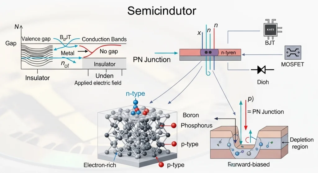
An intrinsic semiconductor is a pure semiconductor material without any intentional impurities or doping. The most common examples are silicon (Si) and germanium (Ge). In intrinsic form, the electrical behavior of the material depends only on its own crystal structure and temperature, not on external impurities. (GeeksforGeeks)
At absolute zero temperature (0 K), an intrinsic semiconductor behaves like an insulator because all electrons are tightly bound in covalent bonds and no free charge carriers exist. When temperature increases, some valence electrons gain enough thermal energy to break bonds and move into the conduction band. This process creates electron–hole pairs (EHPs): free electrons in the conduction band and corresponding holes in the valence band. (Science Facts)
A key feature of intrinsic semiconductors is that the number of electrons is always equal to the number of holes, i.e.,
n = p. (GeeksforGeeks)
Here:
- Electrons are negative charge carriers in the conduction band
- Holes behave as positive charge carriers in the valence band
These charge carriers are responsible for electrical conduction. However, because their concentration is low at room temperature, intrinsic semiconductors have poor conductivity compared to metals. Their conductivity increases significantly with temperature as more electron–hole pairs are generated.
The energy band structure plays an important role. There is a small energy gap (band gap) between the valence band and conduction band. Thermal energy helps electrons cross this gap, enabling conduction.
In summary, intrinsic semiconductors are the purest form of semiconductor materials, where conductivity is controlled only by temperature and the material’s own properties. They form the basic foundation for understanding more advanced extrinsic (doped) semiconductors, which are widely used in electronic devices like diodes, transistors, and integrated circuits.
Features:
- Equal number of electrons and holes
- Low conductivity
- Mostly used in research
Example materials:
- Pure silicon
- Pure germanium
Intrinsic semiconductors are not widely used in commercial electronics.
Extrinsic Semiconductor
Extrinsic semiconductor is doped with impurities.
An extrinsic semiconductor is a type of semiconductor material whose electrical properties are improved by adding a small amount of impurity atoms through a process called doping. Pure semiconductors like silicon (Si) or germanium (Ge) have limited conductivity, but when specific impurities are added, the number of free charge carriers increases, making the material much more useful for electronic devices. Depending on the type of impurity added, extrinsic semiconductors are divided into two categories: N-type and P-type semiconductors. In an N-type semiconductor, pentavalent impurities such as phosphorus or arsenic are added, which provide extra electrons. These extra electrons become the majority charge carriers, while holes act as minority carriers. In contrast, a P-type semiconductor is formed by adding trivalent impurities like boron or aluminium, which create holes due to the lack of electrons. In this case, holes become the majority carriers and electrons are the minority carriers. The ability to control conductivity through doping makes extrinsic semiconductors extremely important in modern electronics. They are widely used in devices such as diodes, transistors, integrated circuits, and many digital systems. By combining P-type and N-type materials, engineers create PN junctions that form the basic building blocks of almost all electronic components. In short, extrinsic semiconductors are specially modified materials designed to enhance electrical conductivity and enable advanced electronic applications in today’s technology.
It is further divided into:
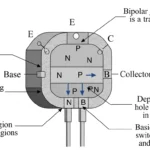
N-Type Semiconductor
An N-type semiconductor is a type of extrinsic semiconductor formed by adding a small amount of pentavalent impurity atoms into a pure semiconductor material such as silicon (Si) or germanium (Ge). This process is known as doping. The purpose of doping is to increase the number of free electrons in the material, which improves its electrical conductivity.
Pentavalent impurities are atoms that have five valence electrons. Common examples include phosphorus (P), arsenic (As), and antimony (Sb). When these impurity atoms are added to silicon, four of their valence electrons form covalent bonds with surrounding silicon atoms. The fifth electron remains loosely bound and becomes a free electron. These free electrons are responsible for conducting electric current.
In an N-type semiconductor, electrons are the majority charge carriers, while holes are the minority charge carriers. This means that most of the current is carried by the movement of electrons. Because electrons are more mobile than holes, N-type materials generally have higher conductivity compared to intrinsic semiconductors.
Even though the material gains extra electrons, it still remains electrically neutral overall. This is because the positive charge of the fixed impurity ions balances the negative charge of the free electrons.
The conductivity of an N-type semiconductor can be controlled by adjusting the amount of doping. More impurity atoms result in more free electrons, which increases conductivity.
N-type semiconductors play a very important role in modern electronics. They are widely used in the manufacturing of diodes, transistors, solar cells, and integrated circuits (ICs). When combined with P-type semiconductors, they form a PN junction, which is the basic building block of many electronic devices.
In summary, an N-type semiconductor is a specially doped material that enhances electron concentration, improves conductivity, and forms the foundation of most electronic components used in today’s technology.
- Doped with pentavalent atoms.
- Electrons are majority carriers.
- Holes are minority carriers.
Common dopants:
- Phosphorus
- Arsenic
P-Type Semiconductor
A P-type semiconductor is an extrinsic semiconductor formed by adding a small amount of trivalent impurity atoms into a pure semiconductor material such as silicon (Si) or germanium (Ge). This process is called doping, and it is used to increase the number of positive charge carriers in the material, improving its electrical conductivity.
Trivalent impurities are atoms that have three valence electrons. Common examples include boron (B), aluminium (Al), gallium (Ga), and indium (In). When these impurity atoms are introduced into silicon, each atom forms covalent bonds with three neighboring silicon atoms. However, since silicon requires four bonds for stability, one bond remains incomplete, creating a vacancy called a hole.
A hole behaves like a positive charge carrier because it can accept an electron from a neighboring atom, effectively moving through the crystal structure. In a P-type semiconductor, holes are the majority charge carriers, while electrons are the minority charge carriers. Most of the electric current in the material is carried by the movement of holes.
Even though holes are created, the material remains electrically neutral overall. This is because the negative charge of the mobile holes is balanced by the fixed positive charge of the impurity atoms.
The conductivity of a P-type semiconductor depends on the level of doping. Increasing the amount of trivalent impurities increases the number of holes, which enhances conductivity.
P-type semiconductors are widely used in modern electronic devices. They play a key role in the formation of PN junctions, which are the basic building blocks of components such as diodes, transistors, solar cells, and integrated circuits (ICs). When combined with N-type semiconductors, they enable controlled flow of current in electronic circuits.
In summary, a P-type semiconductor is a specially doped material where holes act as the primary charge carriers, making it essential for the functioning of almost all modern electronic devices.
- Doped with trivalent atoms.
- Holes are majority carriers.
- Electrons are minority carriers.
Common dopants:
- Boron
- Aluminum
Understanding N-type and P-type semiconductor is essential for learning diode and transistor behavior.
Main Components of Semiconductor Devices
Semiconductor devices contain several important regions.
Conduction Band
- Energy band where electrons move freely.
Valence Band
- Contains bound electrons.
Energy Band Gap
- Energy difference between conduction and valence band.
Small band gap means easier conductivity.
Advantages of Semiconductors
- Small size and lightweight
- Low power consumption
- High efficiency
- Fast switching capability
- Long life span
- Reliable operation
- Suitable for digital circuits
- Easy integration in microchips
Real-world benefit: Modern smartphones are possible because of semiconductor miniaturization.
Disadvantages / Limitations
- Sensitive to temperature changes
- Can be damaged by static electricity
- Lower power handling capacity compared to some older devices
- Requires precise manufacturing
- Expensive advanced fabrication technology
Engineers must use protection circuits when designing semiconductor systems.
Semiconductor Applications
Home Applications
- LED lighting
- Mobile chargers
- Television circuits
- Inverters
Industrial Applications
- Motor control drives
- Power supply systems
- Automation panels
- Welding machines
Communication Systems
- Radio frequency circuits
- Signal modulation
- Network equipment
Modern Technology
- Smartphones
- Computers
- Solar energy systems
- Electric vehicles
- Medical electronics
Semiconductor applications are expanding rapidly in renewable energy and automation.
Comparison Section
Difference Between Conductor, Semiconductor, and Insulator
| Feature | Conductor | Semiconductor | Insulator |
| Conductivity | Very high | Medium | Very low |
| Electron Movement | Free | Controlled | Almost none |
| Example | Copper | Silicon | Rubber |
| Temperature Effect | Resistance increases | Conductivity increases | Minimal effect |
| Main Use | Wiring | Electronics | Protection |
This table clearly explains difference between semiconductor and other materials.
Selection Guide
If you are choosing semiconductor devices, consider:
- Operating voltage
- Current rating
- Power dissipation
- Switching speed
- Temperature range
- Application type
Beginner Tips
- Always check datasheet specifications.
- Use heat sinks for power devices.
- Avoid static discharge damage.
- Maintain safety margin in ratings.
Common Problems & Solutions
Why does semiconductor device overheat?
Cause:
- Excess current
- Poor cooling
Solution:
- Use heat sink
- Reduce load
Why does semiconductor device fail?
Cause:
- Overvoltage
- Static discharge
Solution:
- Use protection circuits
- Follow grounding standards
How to test semiconductor device?
- Use multimeter diode mode
- Check forward and reverse bias behavior
Future Trends
Semiconductor technology is advancing rapidly.
Nano-Scale Devices
- Smaller transistors
- Higher processing speed
Wide Bandgap Materials
- Silicon carbide (SiC)
- Gallium nitride (GaN)
Benefits include:
- High efficiency
- Low heat loss
- Better performance in electric vehicles
Artificial Intelligence Chips
- Used in machine learning hardware
- High computational speed
Future electronics will depend heavily on semiconductor innovation.
Conclusion
Semiconductors are the foundation of modern electrical and electronic technology. Understanding what is a semiconductor helps students and engineers build strong basics in circuit design and device operation.
We discussed semiconductor working principle, types of semiconductors, semiconductor applications, and advantages and disadvantages. You also learned how semiconductors compare with conductors and insulators.
As a beginner, focus on learning atomic structure, doping process, and device behavior. Practical testing and circuit simulation will improve your understanding.
Semiconductor technology will continue shaping the future of communication, energy, and automation systems. Mastering this topic is a big step toward becoming a skilled electrical or electronics engineer.
Keep learning and stay curious.